Furen Technology uses smart sensing mattresses to understand and make caring for the elders warm.
Taiwan is moving towards an aging society, and the demand for long-term care for seniors has increased significantly The invisible killer of long-term care - the fall of an elder is an unspeakable pain for home caregivers and care institutions How to turn every unexpected crisis into the most immediate and warm care is a true test of the adaptability and innovation of smart care In order to make filial piety easier, Foreaider Technology has launched the intelligent sensing mattress Foreaider-Z, a thoughtful auxiliary device that can prioritize the physiological information of the elders, allowing the elders to live with dignity, make up for the lack of care manpower, improve the quality of care, and reduce the cost of care The fall rate reaches more than 25, effectively saving more than 200,000 yuan in care costs per person per year
“To take care of my mother” was the original intention of Furen Technology when it was established in 2018 Luo Yilin, founder and general manager of Furen Technology, said that he has been a caregiver for more than 10 years and recalled that his mother had A patient with severe mental illness spent 20-30 years in a nursing home Because he was reluctant to leave his elderly mother, Luo Yilin decided to shoulder the heavy responsibility of taking care of her In the past, my mother stayed in a nursing home for a long time, which made her unwilling to contact strangers and made her feel insecure about changes in the environment and space This is why Furen Technology "makes filial piety simpler without changing the living environment of the elderly" "Let the elderly live with dignity" as the ultimate goal of the product, we decided to use advanced sensing technology and AI analysis to deliver appropriate care information to caregivers, eliminating the physical and mental torture that caregivers experience when caring for the elderly We look forward to using smart care AI Technology makes interacting with elders easier
Elder falls are the most common accidents that occur when caring for the elderly at home Bed exit warning technology has become one of the important demand indicators for caring for the elderly, Luo Yilin said Insufficient manpower at night is often a headache for the operation of nursing institutions They can only handle daily routine care affairs, but cannot properly manage emergencies or minor symptoms of the elderly, such as falls at the bedside, temporary physical discomfort such as aspiration pneumonia, etc It is a problem that cannot be properly handled by the current ward inspection and shift handover mechanism For nursing institutions, taking bedside falls as an example, a fall may increase the average annual care cost by more than 200,000 yuan per person
In order to build a non-verbal communication bridge between caregivers and care recipients, help care institutions quickly respond to the elderly's physiological and medical information, and improve medical care schedule planning, Luo Yilin and the core team gathered caregivers, doctors, and senior engineers and other professionals, jointly independently developed the "Smart Sensing Mattress" Foreaider-Z to provide homes and care institutions with more thoughtful and high-quality hardware and software AI smart care solutions Helping people without being too strict and helping people without blame is the founding purpose of Helper Technology, which mainly delivers on two levels The first is to put people first and make caring for the elderly a warm interaction In addition, caregivers should have a selfless dedication mentality It has been observed that the cared for may not be willing to express their own needs due to different reasons If the needs of the elders can be grasped through smart care technology, it will not only bring more dignity and dignity to the elders Space can reduce unnecessary communication misunderstandings, make the care process smoother, and reduce care costs
Smart sensing mattress, the caring guardian of the elders, reducing the fall rate by more than 25
In the technological breakthrough of smart sensing mattresses, combined with the physiological micro-motion sensing technology developed by Furen Technology, it uses air pressure changes for physiological sensing and AI algorithms, so that caregivers do not need to replace the original mattress Place the smart sensing mattress with a thickness of less than 1 centimeter under the elder's original mattress, plug it in and connect it to the Internet Wait 3 minutes for the environment parameters to be automatically matched and set, and the pressure on the bed can begin to be accurately detected changes and interpret the actions and behaviors of the elderly
For critically ill and long-term care recipients in nursing institutions, as well as the elderly and infants at home, Furen Technology has launched three versions of smart sensing mattresses, including the smart sensing mattress "Lite version", "standard version" and " Pro version" The Lite version entry-level version, combined with air pressure change sensing technology, can provide home caregivers with relevant identification functions to warn the elderly when leaving bed and inquire about daily routines The OTTALK home care bell APP can be downloaded through the mobile phone, and the caregiver can remotely Set the bed exit warning time and pay attention to the elderly's status of leaving the bed or not, and check the status of work and rest through the mobile phone The standard version, in addition to the bed exit alarm function, can provide caregivers with data measurement status of the elderly's heart rate and breathing during sleep through analog signal calculation technology For the Smart Sensing Mattress Pro version, a three-stage warning function of bed-sitting-up-leaving the bed is specially added, as well as sleep status records such as time in bed, hours in bed, hours of light sleep, hours of deep sleep, hours awake, and number of respiratory arrests and other information, hoping to provide better and more timely services to end customers
In terms of business model, Furen Technology provides small-scale care units with a buyout system that integrates smart sensing mattress software technology In terms of cooperation with SI industry players, the company provides hardware equipment for integration and creates more promotion opportunities through SI channels
For the empirical application of clinical trials, Furen Technology has currently cooperated with Taipei An'an Nursing Home to successively introduce smart sensing mattresses such as Lite, standard, Pro and other functional products into the care environment to provide diversified services for the elderly Intimate and convenient services of intelligent care During the cooperation process, since An'an Nursing Home is a small institution with a shortage of manpower, the bed exit warning function of the smart sensing mattress helps caregivers quickly remotely determine whether the elderly has left the bed or has fallen, effectively reducing the fall rate by more than 25 Through physiological micro-motion sensing technology, it can quickly help caregivers record the elderly's sleep status the previous night, creating a more convenient communication mode and information exchange mechanism between caregivers and family members In addition, the implementation of smart sensing mattresses can help nursing institutions obtain more positive evaluations in the evaluation
Furen Technology develops smart sensing mattresses through physiological micro-motion sensing technology
Smart sensing mattress voice AI recognition reduces the number of people sent to hospital for aspiration pneumonia to less than 5 of the overall number of cases
Optimizing the voice AI recognition establishment mechanism has always been the goal of Furen Technology’s efforts to improve Luo Yilin said that he was very grateful to Furen Technology for having the opportunity to participate in the development plan of AI care services for respiratory diseases under the guidance of the Industrial Bureau and the Information Policy Council painting, and conducted field clinical demonstration at Puli Christian Hospital Through this project, not only the smart sensing mattress uses AI voice recognition and calculation technology to become more sophisticated, but also an AI training optimization framework is established to allow caregivers at Puli Christian Hospital to respond to the elderly’s upper respiratory tract-cough sounds and lower respiratory tract symptoms -The identification and warning performance of heartbeat and respiratory rate changes are more optimized, and the number of people sent to the hospital due to aspiration pneumonia in care institutions is effectively reduced to no more than 5 of the total number of cases in the month It is believed that with the integration of smart sensing mattresses and respiratory disease AI care services, the service is expected to spread to 5 domestic medical institutions this year Luo Yilin said excitedly that not only that, the smart sensing mattress has also been favored by Japanese dealers and conducted product testing In the next stage, business promotion in Japan will be launched
Smart sensing mattress-assisted care institutions reduce the number of people sent to hospital due to aspiration pneumonia
Create the integration of long-term care industry software, hardware and service ecosystem to make care simpler
Although Furen Technology has only been established for 4 years, it took 9 years to complete product technology research and development Luo Yilin expressed his gratitude for supporting and recognizing the company's entrepreneurial philosophy despite limited manpower and resources The guidance and support of the distinguished people as well as the AI Industry Promotion Plan of the Industrial Bureau of the Ministry of Economic Affairs and the Corporate Information Strategy Council For a small start-up like Furen Technology, there are always challenges and learnings in terms of funding, technical issues, obtaining and processing of production materials and parts However, Huangtian pays off its hard work Driven by the ultimate goal of "making filial piety easier", Furen Technology strives to make smart sensing mattresses the first smart care product in Taiwan that uses air pressure sensing physiological information For the original intention of starting a business that emphasizes the orientation of social value, how to make smart sensing mattresses take into account social value while maintaining a win-win and balance of commercial interests is a strategic issue that Luo Yilin must carefully consider when operating the company's products and business development
In the face of business layout, Furen Technology will work hard to stabilize operations and marketing operations in the near future to give back to investors and target customers who have supported the company for a long time In addition, Furen Technology is more active in international business development and product testing in Japan, Vietnam and Poland Regarding the mid-term planning, Luo Yilin believes that the care needs and services of the elderly cannot be completed independently by one industry Furen Technology looks forward to cooperating with more like-minded smart care industry players in the future By gathering the professional energy of each industry, we can build a complete Only with a diverse product chain mechanism can we work together to conquer domestic and foreign markets To this end, Luo Yilin hopes that the company can create an integration of the software, hardware and service ecosystem of the long-term care industry and realize its wish to make care simpler
Looking forward to the future, Furen Technology will hope to move from long-term care to preventive medicine I believe that if preventive medicine is managed properly, it will definitely make a great contribution to saving the cost of long-term care Luo Yilin said that more importantly, it will help the elderly in their later life Halftime enjoys a more understanding quality of care and a bright and hopeful life
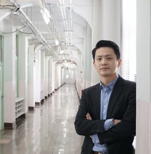
Luo Yilin, CEO of Furen Technology「Translated content is generated by ChatGPT and is for reference only Translation date:2024-05-19」