【2024 Solutions】 AI Defect Intelligent Detection - Energy Reduction Smart Monitoring Solutions
| AIIntelligent Defect Detection-Smart Monitoring Solution to Reduce Process Energy Consumption When there are over2ten thousand chip resistors on a ceramic substrate, how should one quickly detect defects? The answer is:UsingAIto detect。
In the era of rapid technological development, Leike proudly announces significant advances in its laser processing technology, thanks to the innovative applications of artificial intelligence(AI)Leike is committed to integrating advancedAItechnology into laser processing machines, and in2019year, in collaboration with partners, developed the world's first laser machining system that integratesAItechnology, and on this basis further developed in2023year the first ceramic substrate inspection machine that integratesAOI+AI+LASERtechnology.
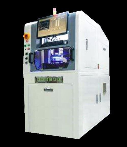
Through the introduction ofAIand machine learning, along with the accumulation of big data samples, the system becomes smarter, which has led to improved product yield within one year5%dramatically reducing the inspection time from originally2minutes/per piece to just20seconds/per piece, drastically lowering inspection costs, enabling efficient initial detection and post-laser marking to reduce waste in subsequent processes, diminishing overall carbon emissions of the site, allowing the automatic generation of detailed inspection reports for data analysis and optimization, which helps increase equipment capacity, reduce human error, enhancing the value of Leike's equipment, and strengthening the international competitiveness of the country's electromechanical industry. | ||||
|
| ||||
| Leike Corporation(Laser Tek)Founded in1988year, and officially listed as a publicly traded company in2002year. Since its establishment, it has become a leading global service provider and manufacturer of electronic packaging materials,SMDElectronic Packaging Materials,SMTinspection equipment, and laser systems.
Leike's general manager, with years of laser integration experience, observed that passive component customers can produce over20With many years of laser integration experience, he observed that the production capacity of passive component customers can exceed10billionSMDcomponents every month, but withSMDcomponents per month. However, as component sizes continue to miniaturize, defect detection during production becomes increasingly challenging. With thousands to millions of components on a single ceramic substrate, and as component sizes decrease and their laser processing positions become smaller, the difficulty of detection increases, making production inspection a critical process.

| ||||
| AOIproblems of yield overkill relying onAIfor oversight, Yet,AOIthe inspection machine is a widespread and mature type, but the high accuracy on the marketAOIuses a technique that captures small images in a single shot and stitches them into a larger image. Although accurate, this method requires more time for small-sizedSMDcomponents, which are more likely to be influenced by environmental factors like lighting and vibration that can cause misjudgments; as a result,AOIyield rate can only be estimated by sampling, and components with poor sampling yield are not removed individually but discarded together with good ones; manual re-inspection not only increases costs, but the lack of unified inspection standards ultimately results in about2%-5%products that are not detected as defective enter the subsequent manufacturing process monthly at least2,000thousands of such defective componentsSMDthat were not initially detected causing ongoing printing and machining inspections in subsequent processes. Regardless of the waste of ink materials and energy, which increases the cost burden, this also accelerates equipment wear and shortens operational life. Each stage of waste increases the site's carbon emissions, unfavorably impacting the company's carbon footprint.
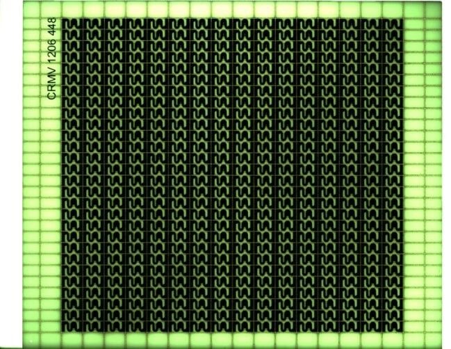
TraditionalAOI High false positive rates in Automatic Optical Inspection (AOI) are a major production issue for manufacturers, particularly in the passive components industry where 'it's better to mistakenly reject a hundred than miss one'—a high standard, often leading to AOI setting extremely high parameters which makes devices overly sensitive. Excessive stringency in data parameter settings can lead to high false positive rates. For instance, if the dirt contamination on passive components resembles the color of the printing layers,AOI the misjudgment rate could reach 7 percent.
Raytek stands apart from otherAOIsuppliers by discarding the stitching of small images or line scanning, effectively preventing data loss and discrepancies caused by hardware or environmental conditions during image processing. It employs a large-array photodetector coupled with custom high-resolution lenses, using specialized imaging for composite processing. Throughout this process, each pixel of the photodetector contains light information captured from various positions. By combining this data, the image resolution and detail are enhanced, reaching a resolution of millions, and with multiple automatic light adjustments, a single shot can manage70*70mmachieving an image resolution up to5umobtaining clear images, then throughSmart-AItechniques for analysis and selection.
| ||||
| Three Innovative Methods to Achieve Rapid InspectionSmart -AI
Raytek's General Manager shares, rapidly implementingAItechnology and reducing inspection computation time, further developingSmart-AIthree major approaches:
Method one, initially useAOIto quickly separate good products from those with controversial defects, focusing the detection on the minority of defective identifications.
Method two, an automated labeling platform simplifies the training issue: by using cameras to collect data from machines, automatic labeling replaces manual labeling, progressively training to improve accuracy. The simpler the problem, the less data needed for training.
Method three,AOIandAIDual-track Advancement: In the smart manufacturing process, relying solely onAOIorAIis not enough to accomplish the task alone, it must be preceded byAOIfirst marking the characteristics, distinguishing between good and defective parts, then usingAIa method for labeling and training. Subsequently, by utilizing a repeating cascade effect, the detection benefits are greater as more training data accumulates,AOIreducing the ratio of errors,AIand gradually increasing the accuracy ratio.
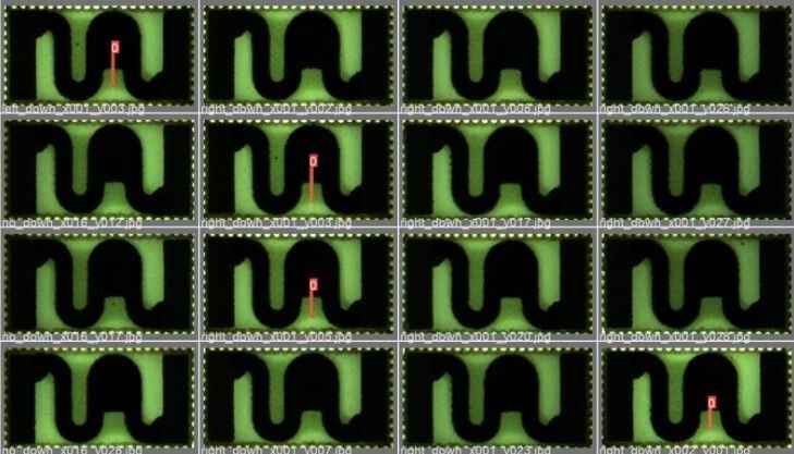
Through three major methods gradually building system reliability, and categorizing data for defect sorting, ultimatelyAIreturning the judgement results to the main system, utilizing laser machining to control truly defective products at the front end of the process, reducing the inflow of defective products into other stations, thus minimizing losses due to repeated tests or reprocessing.
| ||||
| Leading in smart laser equipment, chooseLASERTEKthe right one! Continuously developed by the Taiwanese brand Raytek, combiningAIsmart detection and laser processing equipment to progressively build a smart monitoring solution stack from raw materials, products, testing, laser equipment, etc., aiming at reducing the energy consumption of the production process, implementing semiconductor advancements, /substrates and component processing among other fields, producing equipment products capable of meeting the end-user demands under low carbon conditions, rapidly and with quality products and services expanding both domestic and international markets, enhancing the global competitiveness of localMade in Taiwan(MIT)equipment. | ||||
「Translated content is generated by ChatGPT and is for reference only. Translation date:2024-12-12」
